News
How Is Multilayer PCB Built: Essential Requirements and Standards
Multilayer PCBs are the backbone of modern electronics as they enable complex circuitry and functionality within compact spaces. Their design and production require clear-cut layer alignment and lamination under high temperatures and pressures. This signifies a process demanding attention to material properties, layer placement, electrical connection, and signal integrity.

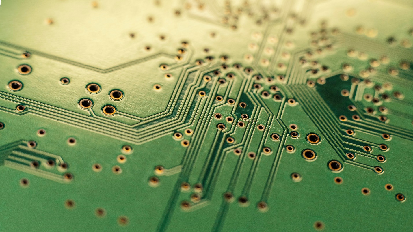
(Copyright image from https://www.freepik.com/free-ai-image/close-up-computer-with-circuit-board-word-circuit-it_42650401.htm#query=Multilayer%20PCB&position=19&from_view=search&track=ais&uuid=8c80dd1a-5d63-4fa1-88a9-45054d016f93">Image By vecstock</a>)
What Are Multilayer PCBs?
As their name implies, this type of PCB consists of multiple layers of nonconductive substrate covered by copper layers with electrical traces, vias, and electrical components. Its production process starts with individual layers processing before they are aligned and pressed together to form an integrated board structure with prepreg, a heat-resistant insulating material acting as a well-functioning adhesive under high temperatures and pressures. After that, intricate via-drilling is performed to afford electrical connections between the layers.
Essential Requirements to Ensure the Quality of Multilayer PCBs
The following are the critical factors in ensuring the quality of multilayer printed circuit boards during production.
l Incoming Material Inspection
In the production of multilayer PCB, incoming material inspection decides the quality of the final product. This step is vital since the choice of materials influences the PCB's electrical properties, thermal performance, and overall stability. YCL King, a custom PCB manufacturer, emphasizes using substrates featuring high TG, halogen-free, high frequency, high CTI, and polyimide for our PCBs. The materials are sourced from reputable brands like Shengyi, ITEQ, Rogers, Isola, Panasonic, Taconic, and Arlon for quality.

(Copyright image from https://www.freepik.com/free-photo/circuit-board-electronic-computer-hardware-technology-motherboard-digital-chip_26698871.htm#query=PCB%20multilayer&position=24&from_view=search&track=ais&uuid=7857c82f-6d67-4e6b-86fb-f78875e0c611">Image by ASphotofamily</a> on Freepik)
l Layer Alignment Precision Using Automated Systems
Precision in layer alignment is critical in manufacturing PCBs made of more than 2 layers. However critical it is, the alignment of multiple PCB layers can be challenging, considering the number of boards and the influence of positioning methods, temperature, and humidity. Therefore, automated systems are brought in to help achieve exact alignment of the numerous layers, which precludes issues like short circuits and guarantees efficient electrical connectivity. Considering our capability to handle complex designs and high-layer-count PCBs, YCL King has employed advanced PCB automation technologies to control the alignment effect better.
l Advanced Etching, Drilling and Copper Plating Techniques
PCB etching can decide the quality of circuit pathways. Hence, it is an essential step in the multilayer PCB manufacturing process and requires specific materials, tools, and safety precautions.
To ensure the reliability and quality of PCBs, especially for the multilayer PCBs with complex and compact designs, YCL King has employed advanced etching, drilling, and copper plating techniques to ensure the desired circuit patterns exposure, precise control of via height and diameter, and copper plating thickness. We offer copper thickness options up to 6OZ for inner layers and 8OZ for outer layers. Regarding the drilling, mechanical and laser approaches are supported with the finished hole size ranging from 0.15-6.3mm for mechanical and 0.076-0.2mm for laser ones. These processes create a PCB's conductive pathways and vias.

(Copyright Image from https://www.freepik.com/free-photo/close-up-green-technological-background_12975350.htm#query=Multilayer%20PCB&position=17&from_view=search&track=ais&uuid=6d714b5a-a744-4dee-a3cf-e6d58462440c">Freepik</a>)
l Robust Inner Layer Bonding Techniques
The strength of inner layer bonding is crucial for the durability and reliability of multilayer PCBs. It involves bonding individual layers into a cohesive unit, so each layer's circuitry is accurately aligned and securely bonded. Undesirable inner layer bonding may cause problems like slipping, delamination, and air bubbles. YCL King can handle complex PCB production's bonding process, including multilayer ones with buried vias and resistors.
l Rigorous Quality Control Processes
Severe tests guarantee that the PCBs of multiple layers can perform their intended functions reliably for consumer electronics or industrial uses.YCL King follows rigorous quality control processes in the PCB manufacturing process. It involves multiple stages of testing, including the x-ray inspection, AOI inspection and other inspection methods, to certify that the PCBs meet the required specifications and perform unfailingly.
l Compliance with Industry Standards
Compliance with industry standards is also a fundamental aspect of PCB manufacturing. YCL King has received certificates of ISO 9001 and ISO13485, demonstrating our pledge to quality control and compliance with industry standards. Such compliance helps preserve consistency in product quality and helps us meet the miscellaneous requirements of different applications in fields like communications, agriculture, and consumer electronics..
For more information about full product assembly essentials, please read From Components to Completion: The Crucial Steps in Full Product Assembly.
Conclusion
Multilayer PCBs, with their convoluted layering and high-density interconnect technology, offer incomparable advantages in innumerable electronic applications. Consequently, selecting a proficient multilayer PCB supplier ensures whole life-cycle product success. YLC King outshines in the multilayer PCB fabrication and assembly business as it boasts rich expertise and comprehensive capabilities ready to serve its clients with boards of exceptional electrical performance and dependability. Start a conversation with us right now to learn more!
CATEGORIES
LATEST NEWS
CONTACT US
Name: Miss Cui
Mobile:+8615727449163
Tel:+86 755 6100 8460
Email:sales@ylc-kingelectronics.com
Add:202 Room F -Building 331 Creative Park, Xixiang Road, Bao’an district, ShenZhen China
